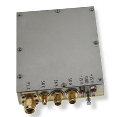
In my time at Quantel, my role was to create a mixed signal ASIC for stabilizing logarithmic amplifiers. These log amps were used in video and radar applications. The issue I had to solve was that log amps are inherently very unstable and given that these amplifiers are used in military applications, they had to work over a wide temperature range. This compounds the issue with stability, making it far worse.
DVLA (Digital Video Logarithmic Amplifier)
The ASIC was defined to provide bias voltages for the amplifiers to stabilize them, based on a temperature measurement from a sensor on the amplifier. Each amplifier was characterized in test and the appropriate bias voltage values were stored in an NVRAM.
Under normal operation, the ASIC ran a process that measured the temperature, compared the temperature value with the NVRAM to get the bias voltage, and output the bias voltage. Inside the ASIC was a small processor (state machine), an I2C interface, some logic, DACs and ADCs.
The size of the ASIC was approx equivalent to about 4500 gates, and was to be rated to military specs; -55 to + 125C. The ASIC was manufactured by Harris Semiconductor (in their fab in Melbourne FL I believe), designed on an Apollo computer design system, using Harris semiconductor FPGA text based design software. (no real graphical interfaces like there is today, or high level languages for definitions)
The only reference I can find to the design of the chip are on the google patents page and this page: Application EP90305332A. These descriptions clearly show the slow speed mixed signal ASIC used for the control and compensation of the log amps.
